Transmission Electron Microscope (TEM)
개요
Transmission electron microscope는 electron beam을 specimen을 통과시켜 이미지를 형성하는 현미경이다. Overall design이 inverted light microscope와 유사하지만 훨씬 크며, 약 0.05 nm의 실용적 분해능을 달성할 수 있어 light microscope보다 200배 이상 향상된 성능을 보인다.
TEM의 기본 설계
전체 구조
크기: 약 2 m 높이의 원통형 column Light microscope와의 유사성: Overall design이 inverted light microscope와 유사 (Figure 9-40)
Figure 9-40: Light Microscope와 TEM 비교
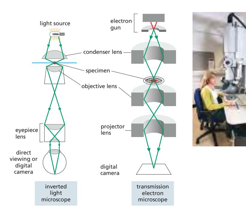
공통 설계 원리 강조:
- Light microscope: Glass lenses 사용
- Electron microscope: Magnetic coils (electromagnetic lenses) 사용 Electron microscope 요구사항:
- Specimen을 vacuum에 배치해야 함
- 약 2 m 높은 원통형 column Inset photograph: 사용 중인 routine transmission electron microscope 보여줌
Electron Beam 생성과 제어
Electron Source
위치: Column 상단 구성 요소: Filament 또는 cathode로 electrons 방출
Acceleration
과정: Nearby anode에 의해 electrons 가속 작은 구멍: Electrons가 통과하여 electron beam 형성
Vacuum의 필요성
이유: Air molecules와의 충돌로 electrons가 산란되는 것을 방지 방법: Column에서 공기를 먼저 pump out해야 함
Focusing
Magnetic coils: Column을 따라 간격을 두고 배치 기능: Electron beam을 focus하며, light microscopy에서 glass lenses가 빛을 focus하는 것과 유사
Specimen 배치와 이미지 형성
Specimen Insertion
위치: Electron beam의 경로에 배치 방법: Airlock을 통해 vacuum 내로 삽입
Image Formation
Scattering: Electron-dense material로 stained 구조에 의해 일부 electrons가 산란됨 나머지 electrons: Focus되어 이미지 형성
Image Observation
Monitor: 이미지를 monitor에서 관찰 가능 Recording: 일반적으로 sensitive CMOS electron detector로 기록
Contrast Mechanism
Dark regions: Scattered electrons가 beam에서 손실되어 어둡게 보임 결과: Dense regions of specimen이 reduced electron flux의 영역으로 이미지에 나타남
Figure 9-39: Electron Microscope의 Resolution
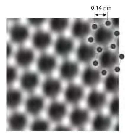 표본: Monolayer of graphene
성취: Individual carbon atoms를 bright spots로 분해
원자 간 거리: 0.14 nm (1.4 Å)
의의:
표본: Monolayer of graphene
성취: Individual carbon atoms를 bright spots로 분해
원자 간 거리: 0.14 nm (1.4 Å)
의의:
- 이러한 resolution은 특별히 제작된 transmission electron microscope에서만 달성 가능
- 모든 lens aberrations가 신중히 correction된 상태
- Optimal specimens 필요
- 대부분의 conventional biological specimens에서는 거의 달성되지 않음 Graphene 특성:
- 단일 isolated atomic plane of graphite
- Carbon nanotubes의 기초
- 육각형 격자 구조의 탄소 원자들
TEM의 분해능
이론적 한계
Electron 파장: 100,000 V accelerating voltage에서 0.004 nm 이론적 resolution: 약 0.002 nm (파장의 약 절반) 이는 100,000배: Conventional light microscope보다 향상
실용적 한계
Electron lens aberrations: Glass lens보다 correction이 훨씬 어려움 결과: 실용적 resolving power는 약 0.05 nm (0.5 Å)로 제한 이유:
- Lens 중심부만 사용 가능
- Effective numerical aperture가 매우 작음
생물학적 표본의 한계
일반적 effective resolution: 1 nm (10 Å)로 제한 제한 요인:
- Specimen preparation 문제
- Contrast 한계
- Radiation damage 성능: 여전히 light microscope보다 약 200배 향상
Field-emission Guns
개선된 Electron Source
특징: 매우 밝고 coherent한 source 효과: Electron microscopes의 성능을 실질적으로 향상
장점
Brightness: 기존 filaments보다 훨씬 밝음 Coherence: 더 일관된 electron beam Resolution 개선: 달성 가능한 resolution 향상
TEM의 장점
1. 매우 높은 Resolution
0.05-1 nm: 생물학적 표본에서 실용적 범위 Atomic resolution: 최적 조건에서 개별 원자 가시화 가능 (Figure 9-39)
2. 광범위한 Magnification
범위: 수천 배에서 수백만 배 유연성: 다양한 크기의 structures 관찰
3. 구조적 세부사항
Ultrastructure: 세포 소기관의 내부 구조 Macromolecules: 대형 분자 복합체 Membranes: Membrane 구조 상세
4. 성숙한 기술
잘 확립됨: 수십 년의 발전 표준화: 준비와 imaging 프로토콜 광범위한 응용: 다양한 생물학적 시스템
TEM의 한계
1. Specimen 제약
고정 필요: 살아있는 세포 관찰 불가 Thin sections: 매우 얇은 sections 필요 (25-100 nm) 복잡한 준비: 복잡한 준비 과정
2. Radiation Damage
Electron beam damage: 고에너지 electrons가 생물학적 재료 손상 누적 효과: 장시간 노출로 구조 변형 Low-dose 필요: 손상 최소화를 위한 낮은 electron dose
3. Contrast 문제
Low contrast: 생물학적 재료는 본질적으로 낮은 contrast Heavy metal staining 필요: Contrast 향상을 위한 추가 단계 Artifacts: Staining 과정에서 발생 가능
4. 2D Projection
3D 정보 손실: Thin section은 2D 이미지 해결책: Tomography나 serial sectioning 필요 복잡성: 3D reconstruction은 복잡하고 시간 소요
TEM vs 다른 Microscopy 기술
vs Light Microscopy:
- TEM: ~0.05-1 nm resolution, 고정 표본만
- Light: ~200 nm, 살아있는 세포 가능 vs Confocal Microscope:
- TEM: 훨씬 높은 resolution, 2D sections
- Confocal: 3D optical sections, 살아있는 세포 vs SEM (다음 섹션):
- TEM: Transmission, 내부 구조
- SEM: Surface scanning, 3D 표면
응용 분야
세포 생물학
Organelles: Mitochondria, ER, Golgi의 ultrastructure Cytoskeleton: Filaments, microtubules의 상세 구조 Membranes: 이중층 구조, membrane junctions
바이러스학
Virus structure: Capsid architecture, envelope Viral assembly: 조립 중간 단계 Host-virus interactions: 세포 내 바이러스
재료 과학
Nanomaterials: Carbon nanotubes, graphene (Figure 9-39) Crystals: Crystal structure와 defects Composites: Material interfaces
병리학
Disease diagnosis: Tissue abnormalities Ultrastructural pathology: 세포 수준 질병 변화 Infectious agents: Bacteria, viruses 식별
기술적 고려사항
Accelerating Voltage
일반적 범위: 80-300 kV 높은 voltage: 더 짧은 파장, 더 나은 resolution, 더 깊은 penetration 낮은 voltage: 적은 radiation damage, 생물학적 표본에 적합
Specimen Thickness
최적: 50-100 nm for biological specimens 너무 두꺼움: Electron scattering 증가, resolution 감소 너무 얇음: 구조적 맥락 손실
Electron Dose
Trade-off: Resolution vs radiation damage Low-dose imaging: Damage 최소화하지만 noise 증가 Cryo-EM: 매우 낮은 dose 사용 가능
요약
핵심 원리: Electron beam을 specimen을 통과시켜 매우 높은 resolution 이미지 생성 Resolution: 약 0.05-1 nm (생물학적 표본), atomic resolution 가능 (최적 조건) 설계: Inverted light microscope와 유사하지만 magnetic lenses와 vacuum 사용 주요 장점: 극도로 높은 resolution, ultrastructure 가시화, 성숙한 기술 주요 한계: 고정 표본만, 복잡한 준비, radiation damage, 2D projection 응용: Cell biology, virology, materials science, pathology
참고 문헌
Chapter 9: Visualizing Cells and Their Molecules, Section: “The Electron Microscope Resolves the Fine Structure of the Cell”, Related Figures: 9-39, 9-40, Related concepts: Biological Specimen Preparation for Electron Microscopy